|
Welcome to Milinda's Home Page |
|
HgSe and Se Semiconductor Nanoclusters in Zeolite |
|
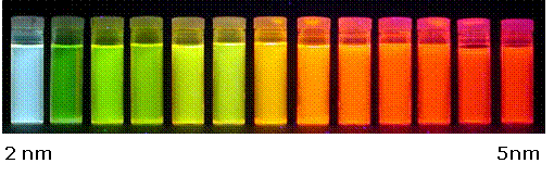
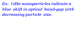
Changing the size of small (10-50 Å ) nanoclusters of semiconductors modifies their optical, electronic, magnetic, thermodynamic, and photocatalytic properties. Such structures are called quantum dots, nanowires or nanoclusters, depending upon their shape and dimensionality. These nanostructures are of great interest for a variety of potential electronic, photochemical and nonlinear optical applications and are necessary for an analysis of the transition from molecular to bulk semiconductor properties. |
|
|
|
RESEARCH INTERESTS & HIGHLIGHTS |
|
Structural and Optical Studies of Semiconductor Nanoparticles |
|
· It is a challenge to produce nanoclusters with a precise, controllable and narrow size distribution. · Zeolite frameworks have the advantage that they constrain the size and shape of encapsulated particles. · Nanoclusters with different sizes and shapes can be synthesized by changing the size and the geometry of the zeolite host lattice. |
|
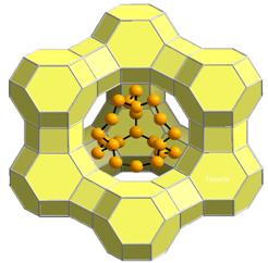
Se semiconductor nanoclusters in Faujasite cages. (001) view |
|
Ex: 1. |
|
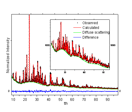
The Rietveld method produces an average atomic structure for such systems. However, due to the influence of the guest atoms, the local structure (especially in the vicinity of the nanocluster) shows deviations from the average. These distortions and the statistical disorder associated with the guest atom sites can give rise to diffuse scattering between super lattice Bragg peaks (Ex.1). The atomic pair distribution function (PDF) technique can be used to model these local distortions and statistical disorder. |
|
Atomic Pair Distribution Function (PDF) Technique |
|
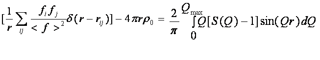
Where, S(Q) - normalized scattering intensity, G(r) = 4πr [ ρ(r) - ρ0 ], Q = 4π Sin(θ)/λ. ρ0 - average number density of the system |

|
For a multi-component system, |
|
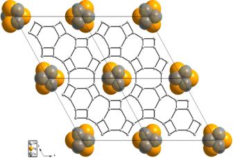
HgSe one dimensional semiconductor nanostructures inside channels of zeolite-L. (001) view. |
|
Ex: 2. |
|
Right : The Rietveld Model to the powder pattern of Se/Nd-Y. Plots show the observed (+), and calculated (-) powder patterns. A difference curve is shown at the bottom of the diagram. The inset shows a log scale version of the graph (Bragg and diffuse scattering). Note that the diffuse scattering is subtracted for the Rietveld refinement. The refined atomic structure is shown on the left diagram |
|
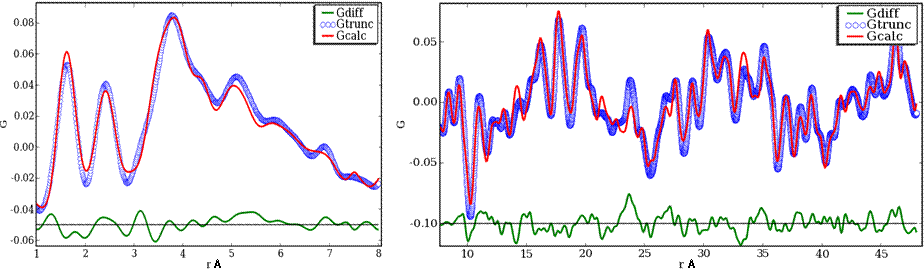
Fourier transform of the total powder diffraction data (Bragg and diffuse) gives the PDF, G(r), |

|
Calculating the PDF directly from the structural model, |

|
Ex: |


|
Milinda Abeykoon Education Ph.D. in Physics, University of Houston, USA, 2006. M.Sc. in Physics, University of Houston, USA, 2003. B.Sc. in Physics, Honors, University of Peradeniya, Sri Lanka, 2000. CV> |
|
Contact Information URL: http://www.uh.edu/~amabeyko/ Address: |