![]()
The two JEOL TEMs (JEOL 2000 FX and JEOL JEM 2010F), operating at 200 kV, have imaging resolution of less than 3 Ĺ. Both microscopes have EDX capabilities but with the capacity to analyze a much smaller area (down to 2 nm). The microscopes also have hot and cold stages so that structural changes may be studied in situ over a range of 77 to 1300K.
Electron Diffraction Patterns
Diffraction patterns show whether a material is amorphous, polycrystalline, or a single crystal
and illustrate the crystalline structure and other features (e.g. defects) of the material.
A diffraction pattern may be obtained from an area as small as 2 nm in diameter.
Imaging Below the Nanoscale
Conventional TEM imaging commonly employs diffraction contrast for studying objects in which details
are more than 15 Ĺ, a typical example is in imaging crystal defects. High-resolution TEM imaging shows
details as small as 3 Ĺ, employing phase contrast and is used in studies of lattice resolution and
short-range order and for amorphous materials.
Observation of Magnetic Domains
Lorenz microscopy images magnetic domains in ferromagnetic materials by defocusing the microscope so
that domains that image dark when underfocused are much lighter when overfocused and vice-versa.
The crystallographic orientations of the domain walls are found by study of diffraction patterns.
TEM JEOL 2000 FX
Transmission Electron Microscope
Capabilities
|
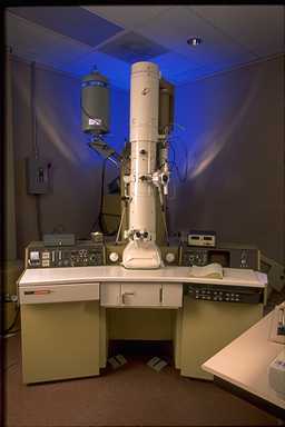 JEOL 2000 FX |
|
| 200Kev, 2.8A resolution | ||
| Link Ultra-thin Window Energy Dispersive Spectrometer | ||
| Link Beryllium Window Energy Dispersive Spectrometer) | ||
| Cryogenic, heating, and tensional sample holders | ||
TEM JEOL JEM 2010F
Field Emission Transmission Electron Microscope
Main Features
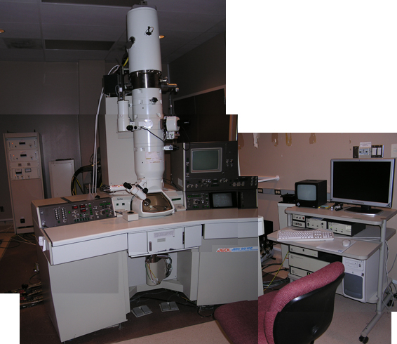
Field Emission JEOL 2010F | ||
Capabilities
|
||