Capabilities
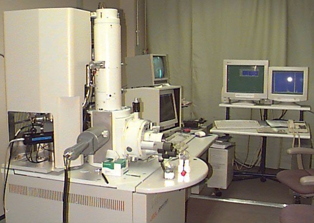
JEOL JSM 6400
X-ray range of 0.15-40 keV
Energy resolution of 55eV
Mineral orientation mapping of thin sections
Kikuchi patterns
JEOL JSM 6400 Scanning Electron Microscope
Capabilities |
JEOL JSM 6400 |
|
| Electron beam Energy: 0.2-40 keV | ||
| Secondary Electron Imaging: resolution of 1.5 nm | ||
| Backscattered Electron Imaging | ||
| Energy Dispersive Spectrometer (EDS): X-ray range of 0.15-40 keV Energy resolution of 55eV |
||
| Electron Back Scattered Diffraction (EBSD): Mineral orientation mapping of thin sections Kikuchi patterns |
||
Imaging at the Nanoscale
The JEOL JSM6330F is a field emission SEM with resolution of 1.5 nm, allowing imaging of nanoscale materials.
Compositional Imaging
Imaging may also be performed with backscattered electrons.
This technique has poorer resolution than secondary electron imaging but yields compositional
information insofar as the backscattered electron intensity depends upon average atomic number.
Phases of different compositions image at different grayscales, allowing grain shapes and sizes
and phase proportions to be determined digitally.
Semi-�Q�u�a�n�t�i�t�a�t�i�v�e� �A�n�a�l�y�s�i�s� �o�f� �I�n�o�r�g�a�n�i�c� �M�a�t�e�r�i�a�l�s
The SEM is equipped with an energy dispersive spectrometer (EDS) that allows rapid compositional analysis.
� �E�D�S� �o�f� �x�-�r�a�y�s� �e�m�i�t�t�e�d� �b�y� �a�t�o�m�s� �i�n� �a� �t�a�r�g�e�t� �u�n�d�e�r� �e�l�e�c�t�r�o�n� �b�o�m�b�a�r�d�m�e�n�t� �r�a�p�i�d�l�y� �p�r�o�v�i�d�e�s� � �i�n�f�o�r�m�a�t�i�o�n�
�a�b�o�u�t� �a�t�o�m�i�c� �c�o�n�t�e�n�t�s� �o�f� �t�h�a�t� �t�a�r�g�e�t�.� �A�l�l� �e�l�e�m�e�n�t�s� �h�e�a�v�i�e�r� �t�h�a�n� �B�e� �m�a�y� �b�e� �a�n�a�l�y�z�e�d� � �s�i�m�u�l�t�a�n�e�o�u�s�l�y�
�o�n� �a� �1�-�3� microns� �r�e�g�i�o�n�.� �O�n�-�l�i�n�e� �d�a�t�a� �r�e�d�u�c�t�i�o�n� �g�i�v�e�s� �r�e�s�u�l�t�s� �i�n� �w�e�i�g�h�t� �o�r� �a�t�o�m�i�c� � �p�e�r�c�e�n�t�a�g�e�s� �w�i�t�h
� �m�i�n�i�m�a�l� �u�s�e�r� �i�n�p�u�t�.�
Crystal Orientation Mapping
The SEM is equipped with an EBSD system for determining crystal structural orientations.
Electron backscattered diffraction (EBSD) uses scattering of electrons that backscatter from the upper
part of a target to construct a Kikuchi pattern demonstrating the crystal structure of the target.
On-line comparison with the theoretical pattern indicates orientation of the target.
Typically, a pattern is obtained and indexed in half a second. A grid of points can be set up that
automatically index the target and draw a crystal orientation map that yields information
about particle sizes, shapes, and orientations. Maps may be determined for any flat
crystalline material-metals, ceramics, and rocks have all been studied in the lab.
The grid size and spacing is chosen to maximize the information yielded. The pattern is derived
from a region 100-500 nm across and 50 nm deep so nanocrystalline materials can be studied.
A 100x100 grid takes about 90 minutes to map.
For more information about this SEM, write to semschedule@uh.edu
If you are a certified user, you can come to our building (HSC202) and book the SEM by writing your name on the schedule posted on the SEM door (room 144)
|
Bring a CD, a memory stick, or a zip disk (100Mb) to retrieve your data files. |
Send mail to apeslier@mail.uh.edu with questions or comments about this web site.
Last modified: May 9, 2006